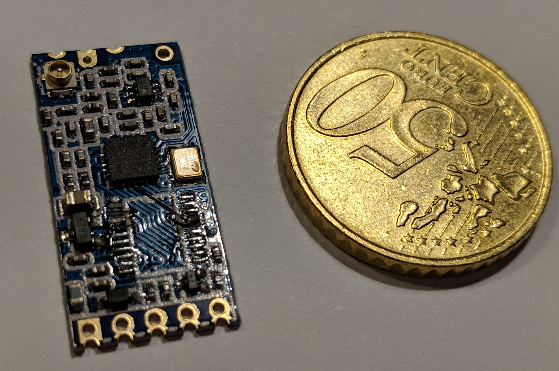
As part of my HC-12 hacking project I needed to acquire the firmware of an STM8 microcontroller that had readout protection enabled.
I was long-time intrigued by fault-injection attacks, most recently triggered by this 35C3 Talk on PS2 Vita Hacking which used voltage glitching to overcome protection measures.
From the STM8 reference manual:
4.5.1: Readout protection
Readout protection is selected by programming the ROP option byte to 0xAA. When readout protection is enabled, reading or modifying the Flash program memory and DATA area [using the SWIM debug interface] is forbidden.
Even if no protection can be considered as totally unbreakable, the readout feature provides a very high level of protection for a general purpose microcontroller.
This looks like a great target for voltage glitching. Thus: challenge accepted! :-)
Glitch Hardware
While others reported doing similar projects with an Arduino, I thought I need the timing precision of an FPGA (and wanted to try writing hardware anyways). Not wanting to spend too much on this, I went with an EPM240, which is a really inexpensive CPLD devboard (~5€) capable of toggling IO Pins at up to 50MHz, which I hoped would be sufficient.
Annoyingly it wasn’t easily usable from Linux, but I eventually managed.
Writing the VHDL was relatively straightforward, but who would have thought that hardware is weird and debugging hardware is a pain (printf debugging is nothing compared to GPIO toggling).
Since the compiling and reflashing part is annoying and slow, I wrote the software to receive a configuration via an UART implementation writing central params to registers:
- trigger polarity
- trigger count
- glitch polarity
- trigger-to-glitch delay
- glitch duration
Glitching Setup
The HC-12 board has a bunch of capacitors which would defeat my glitching goals, so I first tried to unsolder the HC-12 STM8 to an isolated board, but may have broken it in the process (so that’s not recommended).
Unsoldering the MCU |
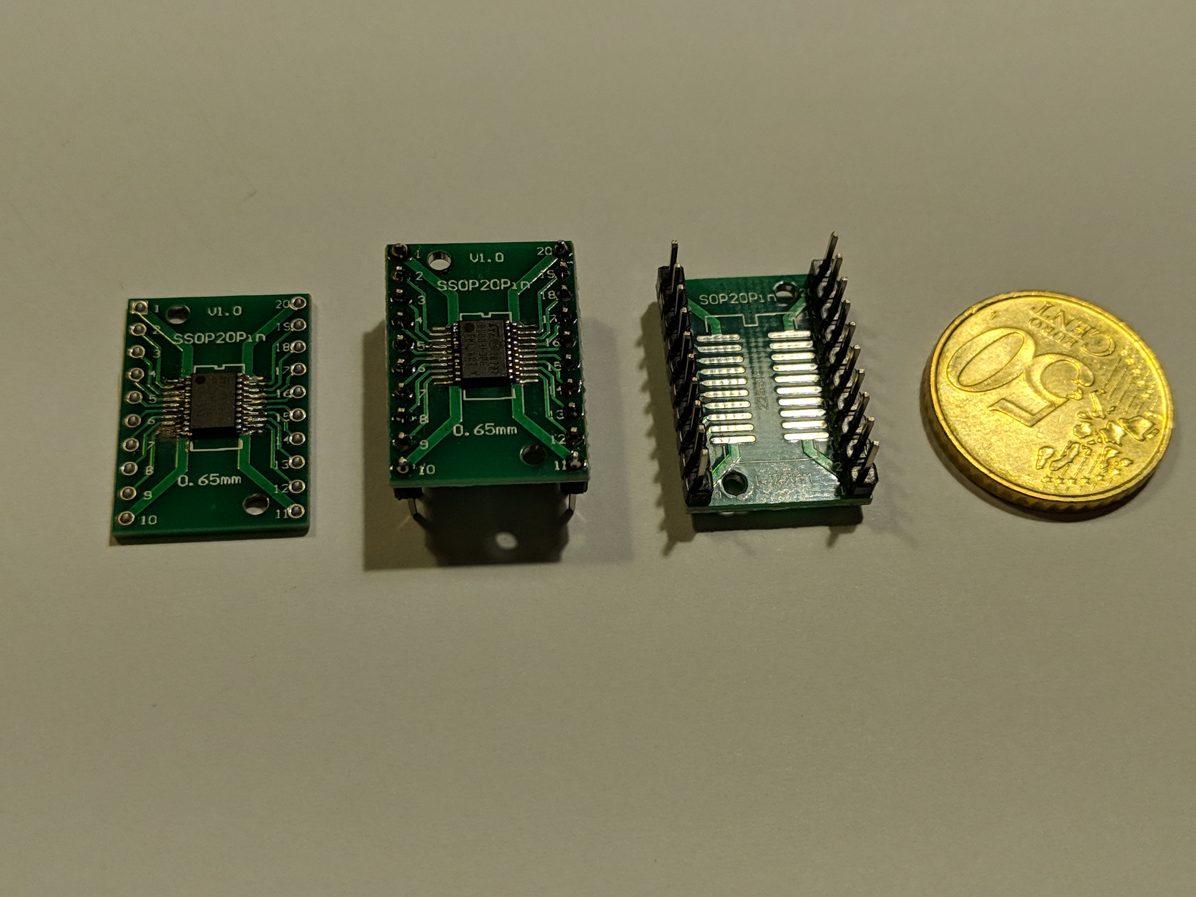
Putting it onto a prototype adapter |
My next attempt was to detach the GND pin from the socket and attach a new wire.
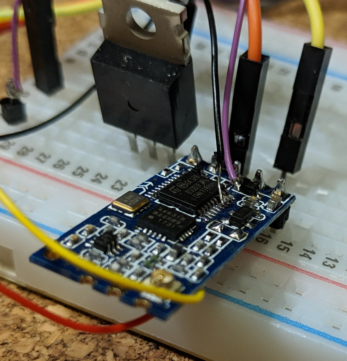
GND Pin detached (overview) |

GND Pin detached (zoomed) |
Here’s what the whole bench looked like:

Glitching Setup
The total of the equipment used is <20€.
My setup seemed to work and I was able to cause seemingly undefined behavior, but I wasn’t able to glitch the option byte loading despite bruteforcing time offset and glitch duration for many nights. I eventually realized that I’m more likely glitching the UART transmission part or my USB-to-serial converter.
Differential power analysis
One of the problems I was facing was that I didn’t really know well when to glitch and trying out all the options. So I devised a power analysis setup on the assumption that the microcontroller consumes more (or less) power when loading option bytes with different amounts of bits set to one.
I borrowed an UT2052 oscilloscope and had to write some linux drivers for it to be able to automate trace retrieval. Then I prepped an STM8 with the readout protection byte set to 0x00, 0xFF and 0xAA. Using the oscilloscope I recorded hundreds of power traces around the reset phase.
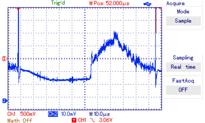
oscilloscope view of power traces around the reset phase
I aligned the traces, averaged them, did consistency checks and removed too noisy ones. The noise graph illustrates the amount of noise within a trace set. Any significant diffs occuring at these points are likely more due to noise than due to different currents during computation of different values.

With that in mind I looked at the difference between the averages of different trace sets. The oscilloscope has a really bad resolution (records <250 bytes @8bits) and thus the SNR is quite bad. Accordingly there are strong artifacts, but there’s also a visible difference. The most promising is around position 150: negative correlation spike followed by a positive correlation spike without a significant event in the noise graph.

Having such candidates clearly helped to refine the search space, even if just saying it’s safe to ignore the first 50μs.
Glitching with success
Trying again with different mosfets and a refined search space I not only tried glitching the VCC and GND pins, but also the exposed voltage regulator PINs, since the datasheet already mentions:
10.3.1 VCAP external capacitor
The stabilization for the main regulator is achieved by connecting an external capacitor CEXT to the VCAP pin.
In hindsight this is a really obvious target, but I was very surprised when my attempts worked on first try within seconds of bruteforcing. Using the now-enabled SWIM debug interface I could simply dump the firmware.
This means: STM8S readout protection is broken (though not really a surprise there).
And if you need to read out the memory of a readout-protected STM8 chip, let me know!